Why Green Silicon Carbide is Used as Abrasive for Silicon Wafer Mortar Cutting
In mortar multi‑wire sawing, thin steel wires carry SiC micropowder suspended in PEG cutting fluid. Material removal is achieved by rolling and ploughing of abrasive grains between steel wires and silicon ingots. The steel wire itself has no cutting capacity. Green silicon carbide is the preferred abrasive for this process for four core reasons.
1. Well‑matched Hardness and Excellent Self‑sharpening Performance (Most Critical)
Monocrystalline silicon has a Mohs hardness of about 7, while green silicon carbide reaches Mohs 9.4‑9.5. Its hardness is sufficient to cut silicon without causing severe subsurface damage like diamond. With moderate brittleness, green SiC particles fracture along cleavage planes under rolling pressure and constantly generate fresh sharp edges (self‑sharpening effect). Particles will not quickly become rounded and blunt.
Black silicon carbide features higher toughness. Its particles hardly break to form new edges. They tend to turn blunt in later cutting stages and easily produce long scratches on wafers.
2. High Purity and Low‑iron Content to Avoid Electrical Contamination
For photovoltaic and semiconductor silicon wafers, iron and magnetic impurities are critical hazards. They may lead to electric leakage, surface stains and reduced cell efficiency. ‑ Cutting‑grade green silicon carbide: SiC ≥99.0%, Fe₂O₃ ≤0.08%, magnetic substances strictly limited. ‑ Black silicon carbide has lower purity (95‑97%) and higher metallic‑iron impurities. It shall not be adopted for silicon wafer mortar cutting. Chemically inert at room temperature, green SiC does not react with PEG cutting fluid or silicon crystals. Residues can be easily cleaned after slicing.
3. Controllable Particle Shape and Particle Size for High‑yield Slicing
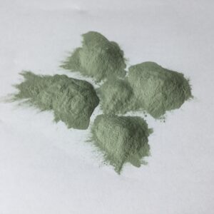
Green silicon carbide forms sharp‑edged crystals. After precise classification to FEPA standards such as F280 / F320, its particle‑size distribution is narrow with over‑sized particles strictly restricted. Oversized grains directly result in deep scratches and chipping on silicon wafers. Mature classification technology stabilizes D50 and particle‑size range, delivering wafers with good flatness, controllable TTV and warpage, suitable for thin‑wafer processing. It also features stable sedimentation in PEG mortar and avoids rapid precipitation and delamination, showing good recycling performance of mortar.
4. Cost‑performance Balance
Diamond has higher hardness yet extremely high cost when used as free abrasive in mortar. Green silicon carbide achieves optimal balance among cutting capability, surface quality and consumable cost. It served as mainstream abrasive in the photovoltaic mortar‑cutting era.