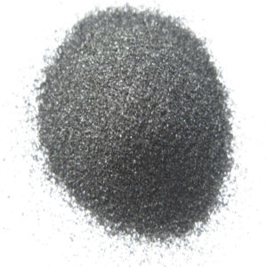
What are the main application areas of silicon carbide wafers?
LED solid state lighting and high frequency devices. The material has excellent characteristics such as band gap, drift speed, breakdown voltage, thermal conductivity, and high temperature resistance several times higher than traditional silicon. Application fields and extreme environmental applications such as aerospace, military industry, and nuclear energy have irreplaceable advantages. The exclusive domestic supplier of silicon carbide single crystals, with an absolute leading position in R&D, technology, market development and commercial operation, has successfully mastered the core technology of 76mm (3 inches) super-large gem-grade SiC2 crystal growth, reaching the international advanced level in 2001 .


