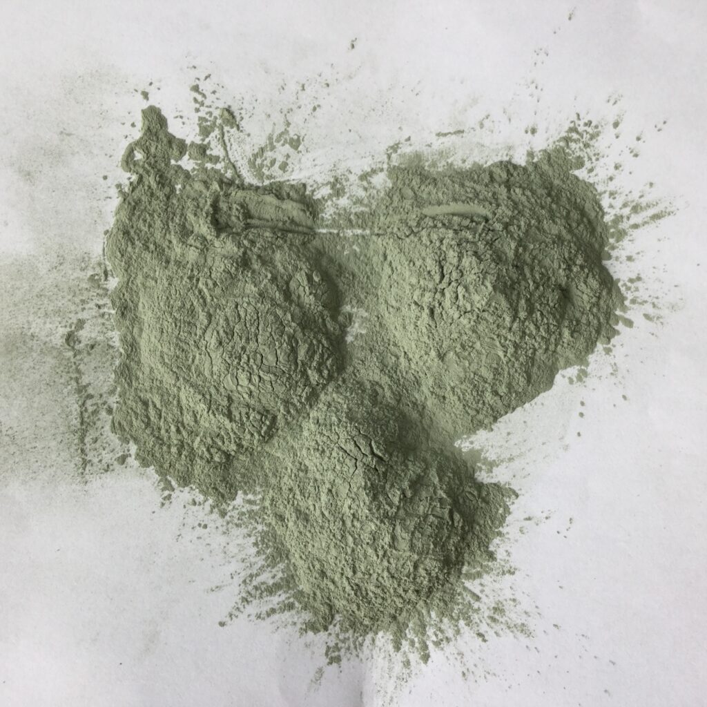
Green Silicon Carbide for Semiconductor Cutting
1. Basic Properties of Green Silicon Carbide
Green Silicon Carbide (chemical formula SiC) is a highly pure (typically ≥99%) variant of silicon carbide. Compared to black silicon carbide, it is harder, more brittle, and of higher purity.
•Extremely High Hardness: With a Mohs hardness of approximately 9.5, it ranks second only to diamond and cubic boron nitride (CBN). This makes it effective in cutting and grinding hard and brittle materials.
•High Brittleness: Microscopically, its particles have sharp edges and break easily when subjected to stress. This allows for the continuous generation of new sharp cutting edges during the cutting process (known as “self-sharpening”), maintaining high cutting efficiency.
•High Thermal Conductivity: This helps dissipate heat during the cutting process, reducing the effects of thermal stress on the silicon wafer.
•Chemical Stability: At room temperature, it does not react with acids or alkalis, ensuring a pure cutting process and preventing contamination of the silicon material.
2. Why choose green silicon carbide for semiconductor cutting?
Semiconductor cutting, especially slicing silicon ingots, places extremely stringent material requirements:
1.Extremely hard cutting material: Although brittle, single-crystal silicon ingots are very hard (approximately 6.5 on the Mohs scale). Effective cutting requires a harder abrasive.
2.Extremely high precision and surface quality requirements: The sliced silicon wafers must be extremely thin (e.g., 100-200μm), with minimal warp and bow, and a controlled surface damage layer. The sharp cutting edge of green silicon carbide enables relatively fine cutting.
3.Cost-effectiveness: Although diamond is a harder material, its cost is significantly higher than that of green silicon carbide. For cutting silicon materials, green silicon carbide strikes the best balance between hardness, efficiency, and cost.
Therefore, green silicon carbide has become an irreplaceable abrasive in traditional slurry cutting technology.
3. Specific Application: Free Abrasive Slurry Cutting
The most classic and once-mainstream application of green silicon carbide in semiconductor cutting is as a free abrasive in the wire cutting process. This technique is known as “slurry wire cutting.”
Working Principle:
1. An extremely fine, high-speed moving metal wire (usually piano wire) is wound around a guide wheel to form a dense wire web.
2. Green silicon carbide micropowder (particle size typically between 5-20 μm) is mixed with a cutting fluid such as polyethylene glycol (PEG) to create a viscous slurry.
3. The slurry is continuously pumped onto the moving wire web.
4. The wire web carries the slurry into the feeding silicon ingot.
5.Under tremendous pressure, green silicon carbide powder particles attached to the steel wire roll, scrape, and cut the silicon ingot, acting like countless tiny “teeth,” gradually chipping away at the silicon material, ultimately slicing the entire ingot into hundreds of thin slices simultaneously.
4. Current Technological Evolution: The Rise of Diamond Wire Cutting and the Challenges of Green Silicon Carbide
In recent years, the semiconductor and photovoltaic industries have undergone significant technological changes: diamond wire cutting (DWS) is rapidly replacing traditional slurry cutting.
•Advantages:
•Extremely fast cutting speed: 3-5 times faster than slurry cutting, significantly improving production efficiency.
•More environmentally friendly: Eliminates the need for large amounts of PEG cutting fluid and SiC powder, resulting in less waste.


